Other ZnO based DMS
The present work is to synthesize and characterize the diluted magnetic semiconductors. The following four series have been chosen for the present research work.
- Zn1-xTixO (x=0.02, 0.03)
- Zn1-xFexO (x = 0.02, 0.04, 0.06)
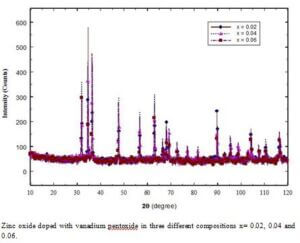
- Zn1-xVxO (x=0.02, 0.04, 0.06)
- Zn1-xNix/2Vx/2O (x=0.02, 0.04, 0.06)
The main objectives of the present work are ;
To prepare ZnO semiconductors by solid-state reaction method (SSR).
To investigate the prepared transition metal doped dilute oxide semiconductor by powder X-ray diffraction for the detailed structural analysis.
To analyze the morphology of the semiconductors by scanning electron microscopy (SEM).
To analyze the elemental compositions of the prepared materials using energy dispersive X-ray spectroscopy (EDS).
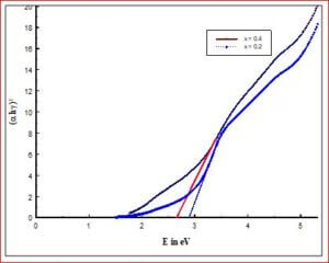
To estimate the optical band gap (Eg) for all the prepared materials by UV-visible absorption spectra by using Tauc plot technique (Wood and Tauc, 1972).
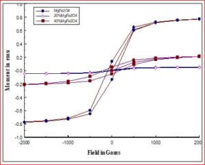
To analyze the magnetic properties of the materials by vibrating sample magnetometer (VSM).
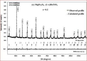
To study charge density distribution for the above mentioned transition metal doped dilute oxide semiconductor using Rietveld (Rietveld, 1969) and maximum entropy method (MEM) (Collins, 1982) using powder X-ray diffraction data.
To correlate the charge derived properties of the transition metal doped dilute magnetic oxide semiconductors with the addition of the dopant with the experimental results.

Magneto-electric composites
Magneto-electric ceramic composite materials
Devices made of Magneto electric (ME) materials are one of the highest priority research topic to develop the next generation of novel multifunctional materials. These systems show the simultaneous existence of two or more ferroic orders, and cross-coupling between them, such as magnetic spin, polarisation, ferroelastic ordering, and ferro toroidicity. Based on the type of ordering and coupling, there is a wide variety of device applications, such as magnetic field sensors, nonvolatile memory elements, ferroelectric photovoltaics, nano-electronics etc. Since single-phase materials exist rarely in nature with strong cross-coupling properties, intensive research activity is being pursued towards the discovery of new single-phase multiferroic materials and the design of new engineered materials with strong magneto-electric (ME) coupling investigated by the scientific ferroics community to develop the next generation of novel multifunctional materials.
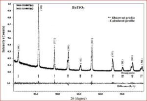
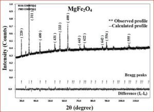
The ceramic material BaTiO3 will be having the dielectric properties which are very useful in a variety of applications. It is a well known dielectric, piezoelectric, ferroelectric material. Ferrites like, CoFe2O4, NiFe2O4, ZnFe2O4, and MgFe2O4 are very useful magnetic materials having variety of applications. They are used in transformer cores, they have low coercivity, high permeability and ferrite cores used for signals have a range of applications from 1 kHz to 300 MHz. Composites of ceramic-ferrites synthesized to enhance the ferroelectric and magnetic properties in a single material. The characterizations (XRD, P-E, M-H, UV-Vis, SEM, EDX, Magnetocapacitance) of the prepared sample gives the nature of the behavior of sample prepared.
Materials interest:
Ceramics, ferrites, ferroelectric materials, Multiferroic materials
- (1-x) BaTiO3 + x CoFe2O4
- (1-x) BaTiO3 + x NiFe2O4
- (1-x) BaTiO3 + x ZnFe2O4
- (1-x) BaTiO3 + x MgFe2O4
Multiferroic materials
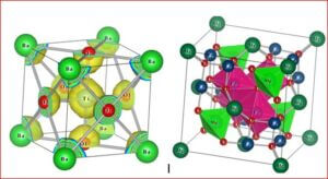
The coexisting states of coupled magnetic and ferroelectric ordering in multiferroic materials makes them interesting for the researchers. The material lanthanum orthoferrite (LaFeO3) is one of the most important multiferroic material due to the simultaneous presence of coupled (ferro/antiferro) magnetic and (ferro/antiferro) electric ordering in that system. LaFeO3 is a ABO3 – typed perovskite like structure, which crystallizes in an orthorhombic phase at room temperature. The perovskite oxide LaFeO3 is known to be a canted G-type wide-gap antiferromagnetic insulator at room temperature with high Néel temperature (TN~740°C). In LaFeO3, La3+ ions are at the corners of the unit cell and the Fe3+ ion lies at the centre of octahedron formed by six O2- ions.
The structure, size, physical and chemical properties of LaFeO3 are strongly influenced by the choice of synthesis method along with the substitution of divalent or trivalent or tetravalent ions at the La site of host lattice in LaFeO3. Since LaFeO3 exhibits significant physical and chemical properties, it is of great importance to be used in many branches of modern technologies such as solid oxide fuel cells, photocatalyst, chemical sensors, non-volatile magnetic memory devices, ultrasensitive magnetic read heads of modern hard disk drives, novel spintronic devices, and multistate memories etc.,. To understand the physical and chemical properties of LaFeO3, the electronic distribution and the nature of chemical bonding between the atoms in the unit cell are essential. Therefore, this research work is aimed at synthesis, characterization and charge density distribution analysis of pure and doped LaFeO3 multiferroic materials such as i) La1-xAlxFeO3 ii) La1-xCexFeO3 iii) La1-xSrxFeO3 and iv) La1-xZnxFeO3 . The multiferroics La1-xAlxFeO3, La1-xCexFeO3, La1-xSrxFeO3 have been synthesized through high temperature solid state reaction method and La1-xZnxFeO3 has been synthesized by chemical co-precipitation method.
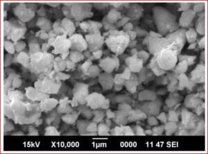
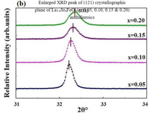
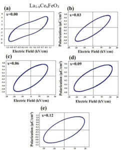
The structural analysis of the synthesized multiferroics has been done through Rietveld refinement process using JANA2006 software. The charge density and interatomic bonding analysis have been done through high resolution maximum entropy method (MEM) by employing the softwares PRIMA and VESTA. The optical behaviour, polarization behaviour, magnetic ordering and electric ordering have been correlated separately with the experimental charge densities which have not been done so far.
Research Materials studied
Ceramic materials, multiferroic materials, dielectric and magnetic materials
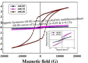
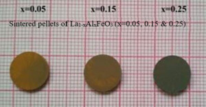
La1-xCexFeO3 (x=0.00, 03, 0.06, 0.09 and 0.12) (LCFO) La1-xZnxFeO3 (x=0.00, 0.05, 0.15 and 0.25) (LZFO) La1-xAlxFeO3 (x=0.05, 0.15 and 0.25) (LAFO) La1-xSrxFeO3 (x= 0.05, 0.10, 0.15 and 0.20) (LSFO)


Piezoelectric Materials
Piezoelectric materials are nowadays widely used as transducers, actuators or sensors due to their excellent piezoelectric properties. Piezoceramics are found in many applications as in ultrasonic transducers, mobile phones, etc. The solid solution of lead zirconate titanate (PZT) is one of the most frequently studied ferroelectric materials, which is useful in actuating and sensing applications. Although, lead-based perovskite ceramics are dominating the markets of both the piezoelectric and the ferroelectric devices, the toxicity of lead has raised serious environmental issues. Hence, the growing demand for replacing these lead-based piezoelectrics has paid more focus on the development of efficient lead-free systems.
More than a decade of intense research provides primordial interest for developing lead-free ceramics as an alternative of lead-based materials in many technological applications. Amongst the several systems investigated, BaTiO3, Na0.5Bi0.5TiO3 (NBT) and (Na, K)NbO3 (NKN)-based systems are the most promising lead-free ceramics. To replace the lead-based piezoelectrics, a lot of studies related to lead-free piezoelectric materials have been conducted.
The research topic in our work fuscous the preparation of the lead-free ceramic solid solutions and characterization of them using XRD, SEM, EDS, UV-Vis, dielectric, ferroelectric, piezoelectric measurements. The crystal structure of these ceramics has been analyzed using charge density route and correlated with the other experimental measurements, primarily the piezoelectric measurement. In this context, the following five series of lead-free piezoceramic (solid solutions) have been chosen for the present work as follows;
Research Materials studied
(1-x)(Na1-yKy)NbO3-xBaTiO3, (x=0.1, 0.2; y=0.01, 0.05) (1-x)(Na1-yKy)(Nb1-zSbz)O3-xBaTiO3, (x=0.1, 0.2; y=0.03, 0.05; z=0.05, 0.1) (1-x)(Na0.5Bi0.5)TiO3-xBaTiO3, (x=0.00, 0.04, 0.08, 0.12) (1-x)(K0.5Bi0.5)TiO3-xBaTiO3, (x=0.00, 0.08, 0.12) (1-x)Ba(Zr0.2Ti0.8)O3-x(Ba0.7Ca0.3)TiO3, (x=0.4, 0.5, 0.6)


DMS - Si & Ge based
The silicon (Si) and germanium (Ge) based diluted magnetic semiconductor (DMS) materials considered here are;
Research Materials studied
Ge1-xMnx (x = 0.04, 0.06, 0.10)
Ge1-xVx (x = 0.03, 0.06, 0.09)
Ge1-xCox (x = 0.03, 0.06, 0.09)
Si1-xMnx (x = 0.02)
Si1-xNix (x = 0.03, 0.06, 0.09, 0.12)
The doping of Mn in the host Ge matrix has been confirmed from the changes in the lattice parameters. The contribution of the intermetallic domains to disorder of the lattice has been confirmed by the observed powder X – ray intensity peaks. The formation of Mn – poor Ge8Mn11 is preferred when x = 0.04 while formation of both Mn – poor Ge8Mn11 and Mn – rich Ge3Mn5 is preferred for higher concentrations of the dopant. A compression of lattice has been observed when x = 0.04 and expansion of lattice has been observed when x = 0.06. This is due to the hybridization of d orbital of Mn with p orbital of Ge that causes local magnetic moment of Mn atom in the Ge matrix. This magnetic moment increases the mixing of the orbitals and thus affects the structural parameters of Ge1-xMnx. The formation of the intermetallic domains, Ge3Mn5 and Ge8Mn11 increases with the dopant concentration and hence, the disorder in the system increases. Therefore, from our observation, x = 0.06 is suggested as the maximum possible dilution for the preparation of DMS Ge1-xMnx.


Resarch Materials
The following manganite structured materials have been considered.
Research Materials studied
- (Co, Mn) doped (La, Ca) based chromites-(La0.8Ca0.2)(Cr0.9-xCo0.1Mnx)O3
- (Co, Fe) doped (La, Ca) based chromites-(La0.8Ca0.2)(Cr0.9-xCo0.1Fex)O3
- (Co, Cu) doped (La, Ca) based chromites-(La0.8Ca0.2)(Cr0.9-xCo0.1Cux)O3
- La1-xCaxMnO3 manganites
- La1-xSrxMnO3 manganites


Dielectric ceramics – Titanate based
Importance of barium titanate (BaTiO3)
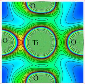
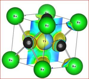
Recent technological improvements impose an increasing demand of the novel ceramic materials with enhanced material performance. Barium titanate (BaTiO3) has been one of the highly explored ferroelectric lead-free ceramic materials since its discovery in 1940s. It has a simple crystallographic structure and has found extensive uses in the electronic and communication industry. Barium titanate and barium titanate derived compounds have become the most promising ceramic materials to reach all the practical requirements. In BaTiO3, the dielectric and ferroelectric properties arise from the covalent hybridization between Ti and O ions. BaTiO3 is used as first ever piezoelectric transducers, like sensors and actuators, due to its unique ability of coupling mechanical and electrical displacements. BaTiO3 derived materials offer high pressure per density ratio for actuator type devices. They are also environment friendly with chemical stability compared to other systems. The widest range of applications are, multilayer ceramic capacitors (MLCCs), piezoelectric sensors, transducers, actuators, non-volatile random access memories (NVRAM), ferroelectric random access memories (FeRAM), dynamic random access memories (DRAM), electro-optic devices etc. The positive temperature coefficient of resistance (PTCR) makes BaTiO3, one of the highly wanted electro ceramic materials among the various known ceramic materials. BaTiO3 has been synthesized and investigated for precise electronic structure, chemical bonding, electron density distribution of five differently doped barium titanate (BaTiO3) lead-free dielectric ceramic materials with various dopant compositions. Various effects such as, structural modification, average grain size, optical band gap variation, chemical composition and morphological changes due to dopants have been studied. In order to achieve the objectives, the following tasks have been carried out.
Synthesis of five different doped BaTiO3 ceramic solid solutions has been carried out as follows;
Research Materials studied
BaTi1-xZrxO3 Ba1-xLa2x/3TiO3 BaTi1-xCexO3 Ba1-xSrxTi0.9Zr0.1O3


Ferrite materials
Ferrite materials
One can find applications of ferrite materials from a simple permanent magnet to most sophisticated equipments in medical fields. Ferrites have an important advantage over other magnetic materials. The oxygen ions in the ferrites insulate the metal ions in the compounds thereby increase the resistivity which leads to decrease in the eddy current losses. High frequency devices, used in several applications, require materials with low eddy current loss and hence, ferrite materials attracted researchers for the last three decades and still continue to do so. Moreover the magnetic property of ferrites can be “tailored” by varying the distribution of cations over the available tetrahedral (A) site and octahedral (B) site in the unit cell. The cations, in micrometer regime have their “own” preferred sites (A or B sites) of occupation in the unit cell, whereas in nanometer regime, this occupation constraint is not strictly adhered and hence, cation distribution can be “tailored”. Methods of preparation and dopants play a major role in bringing down the particle size to nano scale.
Understanding the bond strengths requires an intense knowledge on charge density distribution. There is not much work has been reported so far on bond strengths between atoms at A-site and B-site of ferrites by deploying maximum entropy method (MEM) techniques in the unit cell of ferrites. This motivated researchers to carry out intense research on the bond strengths and other characterization on ferrites. The physical and chemical properties of atoms or molecules mostly depend on the charge density distribution, bond strength etc. Hence, the following samples were synthesized and studied for their bond strength between various sites (A-A, A-B and B-B sites) using MEM.Ni0.5Zn0.5Fe2O4.
Research Materials studied
Ni0.5Zn0.5Fe2O4 - sintered at 700°C to 1400°C. Mn0.4Zn0.6Fe2O4 Co0.4Zn0.6Fe2O4 Ni0.53Cu0.12Zn0.35Fe2O4 Mg0.2Cu0.3Zn0.5Fe2O4 Ni0.8Zn0.2Fe2O4 NiFe2O4


NLO
Non Linear Optical (NLO) materials
PbMoO4 has been the subject of extensive study because of its potential applications, such as photoconductivity, luminescence, thermo-luminescence and photo catalysis. A study on electron density distribution of PbMoO4 is not available in the literature. Therefore, an attempt has been made in this study to investigate the electron density distribution using the X-ray powder diffraction data.
Lithium niobate (LiNbO3) is one of the most investigated NLO materials for widespread and promising applications in non-linear optics (e.g., parametric amplification, second-harmonic generation, holographic data storage, and optical information processing). LiNbO3 can be utilized as a high temperature acoustic transducer, such as an accelerometer for jet aircraft because of its high Curie temperature (Tc =1210° C). The existence of threshold effect with regard to magnesium doping level in LiNbO3 single crystal has been confirmed by measuring IR absorption and photoconductivity by. It was reported that the high-speed and low-noise holographic storage with considerate diffraction efficiency has been achieved in LiNbO3 crystal by using two dopants Mg and Fe (i.e., Mg:Fe:LiNbO3). LiNbO3 crystals doped with magnesium might lead to the formation of defects and suppress the optical damage. The holographic storage properties of the LiNbO3 crystal can be greatly improved by doping with ZnO. In spite of the fact that the single crystals of LiNbO3 have several applications, still there are restrictions because of their high cost and difficult fabrication. In our work, an attempt has been made to study the electron density distribution, the bonding between the atoms and local structure of LiNbO3.Ce doped gadolinium gallium garnet (Ce:Gd3Ga5O12) The early work on non-linear optical materials showed that gadolinium gallium garnet (Gd3Ga5O12, GGG), is a subject of intense research for the past three decades, because of its interesting properties, such us chemical stability, mechanical hardness, good thermal and optical behavior. It was reported that the GGG single crystals can be used as an appropriate substrate for yttrium iron garnet (YIG) and YIG-like magneto-optical epitaxial film in the field of integrated optics. Neodymium doped GGG single crystal (Nd:GGG) can be regarded as a promising and key material for solid-state high power heat capacity laser. A method to increase the lattice parameters of GGG crystal employing coupled substitution of gallium by magnesium and zirconium, and gadolinium by calcium has been reported. A study on electron density distribution of Ce:Gd3Ga5O12 is not available in the literature. Hence, this material is chosen for the electron density analysis in this work.Calcite (CaCO3) Calcite (CaCO3) is one of the most probed NLO materials for widespread and promising applications. It was reported that calcite crystal has strong uniaxial anisotropic nature. Numerous studies are available on the pressure induced phase transition behavior of CaCO3. It was reported that CaCO3 undergo phase transitions from calcite I to calcite II (slightly denser phase), and from calcite II to calcite III (significantly denser phase), at a pressure of 1.44 GPa and 1.77 GPa respectively. It was reported that the above mentioned phase transitions occur at 1.45 GPa and 1.74 GPa respectively at room temperature. It was also reported that the same phase transitions occur at 1.5 GPa and 2.2 GPa respectively. A comprehensive non-destructive methodology for the simultaneous quantitative determination of the calcite crystal phases using the Fourier transform Raman spectroscopy (FT-RS) was reported by Christos and Nikos (2000). The present work on calcite (CaCO3) can be considered as a clear and precise attempt in visualizing the electron density distribution and bonding nature in the unit cell.
Research Materials studied
PbMoO4; LiNbO3; Ce:Gd3Ga5O12; CaCO3; Yb:CaF2; Al2O3; Cr:Al2O3; V:Al2O3


Nano Semiconductors
Nano Semiconductors
Semiconductors have an electrical conductivity to a degree in between the metals and insulators and it can be used mainly in the field of electronics. When the particle size of the semiconducting material is reduced, it can give unexpected electrical and optical characteristics. Due to the different characteristics of nano semiconductors than micro particles, most of the research works are being concentrated towards nano semiconductors in the recent decades. The band gap of the nano semiconductors can change with the reduction of size of the particles and the edges of the bands split into the different energy levels. Specifically, this phenomenon results from electrons and holes being squeezed into a dimension that approaches a critical quantum measurement which is called exciton Bohr radius. But, researchers have also found band gap increase in some nanomaterials having sizes far beyond the quantum confinement regime. The band gaps have a major influence on the properties of the semiconductors including optical absorption, electrical conductivity and index of refraction.
Nano-sized oxide semiconductors like ZnO, TiO2, SnO2, La2CuO4 etc. are very promising semiconductors because they have easily adjustable electronic properties. ZnO nanostructures can be implemented in the field of optoelectronics, sensors, transducers and biomedical applications. Also, ZnO nanostructured semiconductors have been used as UV blocker in sun screens. Nanostructured SnO2 material has a wide band gap with numerous applications as gas sensors, transparent conducting electrodes, transistors etc. Tin oxide is an n-type semiconductor and the sensor conductivity of SnO2 increases in the presence of reducing gases (CO) and decreases in the presence of an oxidizing gas (O2). Also, the use of nanomaterials for solar energy conversion to environmental cleanup has been one of the most active research areas in photo catalysis. Titanium dioxide (TiO2) is considered to be an ideal semiconductor for photo catalysis because of its high stability, low cost and safety toward both humans and the environment. Study on titanium dioxide nanotube layer is an active field of research concerning antibacterial efficacy, orthopedic, dental surgery, drug delivery platforms, tissue regeneration and implants. The present thesis work has been carried out on the Synthesis and characterization of nano semiconductors. Some nanostructured semiconductors have been prepared and studied in this doctoral work. The following materials have been studied in this work.
Research Materials studied
1. ZnS nanoparticles; 2. TiO2 nanowires and nanoparticles; 3. Nano-NiO; 4. ZnO:Ga nanostructures; 5. Mn doped SnO2 nanoparticles; 6. Mn doped CeO2 nanoparticles; 7. Mn stabilized cubic zirconia nanostructures


Thermoelectric Materials
The thermoelectric phenomenon is a direct energy conversion process by electrons in the solids and this phenomenon has various advantages in harmony with our environment. The devices based on thermoelectric property have various advantages over other techniques and are “environmentally green”. The thermoelectric mechanism is not macroscopic, but depends on the microscopic phenomena like crystal structure, nature of the bonding between constituent atoms, lattice thermal vibration effects, electron density distribution between the atoms and the local structural distribution between the nearest neighbor atoms.
The development of any country relies on the research and development, production in large scale and usage of the advanced novel materials. In this context, the thermoelectric materials have their own stand because of their major device applications. Also, the important crises like global warming, ozone depletion and heavy oil shortage can be solved by the usage of effective thermoelectric materials. The global warming can effectively be reduced by the proper usage of thermoelectric devices based on thermoelectric phenomena, because these materials have the ability to convert waste heat energy into usable electrical energy. The applications include the conversion of waste heat into electricity in micro/nano integrated chips to large scale industry like steel plants. The ozone layer is depleted, because of the ozone holes partly produced by the chloro fluro carbons (CFC) emitted from the household refrigerators. The usage of CFC can be completely eliminated by using the alternate refrigerator called thermoelectric coolers. Around 65% of fuel energy is wasted as heat in almost all diesel powered vehicles. This waste energy can be converted into useful electrical energy and stored in auxiliary batteries. Thus the fuel efficiency can be enormously increased.
The thermoelectric phenomenon and technology have attracted a renewed interest from the viewpoint of increasing needs of environment-friendly energy sources. In the last decade, new thermoelectric materials have been searched extensively, some of which have better thermoelectric properties than the conventional thermoelectric materials. From the viewpoint of basic science, the thermoelectric power depends on entropy change mediated through electrons. This is more or less a controversial terminology because the entropy and heat are concepts in the macroscopic world, whereas the electron is a concept in the microscopic world. Thus, thermoelectric effect is laying a boundary between microscopic and macroscopic worlds, which will give a new insight or direction to condensed matter physics.
Research Materials studied
Mg2Si; PbTe; Bi80Sb20; Bi2Te3; Sb2Te3; Sn1-xGexTe; InSb


DMS - ZnO based
O-DMS (Oxide based DMS) materials have created interest due to the possibility of inducing room temperature ferromagnetism. O-DMS materials are essential materials in spintronic devices. The study of local structural fluctuation and electron density distribution may help in imminent understanding the nature of bonding and charge transfer etc. The results of localized structure of the material with varying dopant concentration may pave way for new spintronic devices. The main objective of this work is to investigate the growth, physical and X-ray characterization of samples having room temperature ferromagnetism and semiconducting properties. The growth of ZnO doped with transition metals like V, Ni, Fe and Ti and mixed systems (possibility of RT FM) has been accomplished. Melt growth technique has been used. Solid state reaction technique offers several advantages such as low cost, easy controlling of the total dopant amounts, and facility of producing bulk amounts of materials. The growth has been accomplished using a well-planned temperature control programme. The quality of the grown samples have been checked by X-ray methods. The impurity levels have been estimated using SEM/EDAX (Energy Dispersive Analysis of X-rays). Powder X-ray data – to study structural changes have been used to determine the compositions of the dopant atoms. The magnetic susceptibility measurements, M Vs H, M Vs T to analyze the AFM, FM transitions have been done.
Optical band gap studies have been undertaken in-order to measure the optical properties of ZnO.
The samples studied are as follows;
Research Materials studied
Manganese doped Zinc oxide (Zn1-xMnxO); Chromium doped Zinc oxide (Zn1-xCrxO); Cobalt doped Zinc oxide (Zn1-xCoxO); Cobalt and Manganese co-doped Zinc oxide (Zn1-2xCoxMnxO); Magnesium doped Zinc oxide (Zn1-xMgxO)


Metals
Metals and alloys
The development of improved metallic materials is a vital activity at the leading edge of science and technology. Metals offer various combinations of properties and reliability at a cost which is affordable. They are versatile because subtle changes in their microstructure can cause dramatic variations in their properties. An understanding of the development of microstructure in metals, rooted in thermodynamics, crystallography and kinetic phenomena is essential for the materials scientist.
Alloys can blend the properties of two or more metals to create a hybrid metal that is more cost effective, stronger, more durable, and overall better suited to its intended purpose than the pure metals used to create the compound. With emerging requirement of designing new materials capable of sustaining high strain rate and severe operating conditions with reduced wastage of cost, energy, and material, it has become an important issue to develop full understanding of the nature of enhanced mechanical properties of the materials. New materials that can be tailored for individual applications are always in a constant demand. As the range of uses for powder metallurgy, hard metals and electronic materials expands, customer requirements are causing materials companies to come up with new products that have the required properties.
Metals and semiconductors play an important role in the present world as evidenced by their variety of applications. Hence, a study on some important metals, alloys and semiconducting systems is essential in terms of the local structure and the average structure which are completely different. The usual methods of analysis using structural refinement of X-ray or neutron data will give only the average structure of the materials under investigation. The studies on the local structure of materials seem to be rare because of the complexity of the problem. There is only limited information available on the investigations of materials in terms of the local structure. Numerous research papers are being published every year based on powder as well as single crystal X-ray diffraction data. The structures reported using those data are only average structures. Since, the analysis of local structure needs highly precise data up to maximum possible Bragg angle, accurate refinement of the data is limited. Due to the complexity of the problem, tasks of acquirement of precise X-ray data from the samples, and the computational incapabilities, local and average structural analysis has not been much explored. Atomic ordering is closely related to the materials’ electronic and magnetic properties. Although the physical properties of alloys are closely related to their electronic structures, studies on the charge transfer and hybridization of the electronic states are still insufficient.
In our investigation, apart from pure metals, the local and average structures of doped metals and alloys are carried out with various doping concentrations. The average structure has been studied using both single crystal and powder X-ray diffraction data in some cases. The bonding and electron density distribution of the host as well as dopant atoms has been studied using tools like MEM (maximum Entropy Method) and multipole analysis. For powder analysis, Rietveld refinement technique (for average structure) and Pair Distribution Function (for local structure) have been used. Effects on the electron density distribution of ball milling has been analysed in this work.
The metals and alloys analysed are Sodium (Na),Vanadium (V),Magnesium (Mg), Aluminium (Al),Titanium (Ti), Iron (Fe), Nickel (Ni), Copper (Cu), Zinc (Zn), Tin (Sn), Tellurium (Te), cobalt aluminium (CoAl), nickel aluminium (NiAl), Iron nickel (FeNi), nickel chromium (Ni80Cr20) , Sodium chloride with iron impurities (Na1-xAgxCl), Aluminium, with iron impurities (0.215 wt % Fe and 0.304 wt % Fe), doped and undoped semiconductor gallium arsenide (n – GaAs).
Research Materials studied
Na; V; Mg; Al; Ti; Fe; Ni; Cu; Zn; Sn; Te; CoAl; NiAl; FeNi; Ni80Cr20; Na1-xAgxCl; Aluminium with iron impurities (0.215 wt % Fe and 0.304 wt % Fe); n-GaAs


DMS - Oxide based
The present work explores growth, effect of doping magnetic materials (Mn, Co, Ni) in to the host semiconducting material and its electronic properties. The main results of this work include (i) an exhaustive study on the Rietveld analysis to analyze the structure properties of the material by X-ray powder diffraction data. (ii) The topology of the charge density in the crystal analyzed for the understanding the expansion and contraction of the atoms in doped magnetic material. (iii) the high resolution electron density studies carried out by MEM (maximum entropy method) to reveal infinitive information on their magnetic behavior. (iv) the local and average structures from atomic pair distribution function (PDF).
Many research works have already been reported, however the charge density studies from X-ray data as in the present work have not been established previously. In magnetic semiconductors, the charge is transferred to the intermediate space and this charge actually holds the core of the atoms together in the bond. It is an interesting thing to analyze this transfer of charges quantitatively as well as qualitatively and hence this study forms the basis of the present research work on some of the magnetic semiconductors.
The bonding in the magnetic semiconductor is very interesting to deal with, as to how the charge is transferred according to the concentration of transition metal doping, but, a fraction of the charge is always left with the host ion or given excessively to the neighbor while bonding, or sometimes spilled over the space, which makes the ions to have slight aspherical charge density distribution. This is the reason why the ions are expected to behave electrostatically the same way, as it was before bonding. Our investigation is based on the study of this behavior qualitatively and quantitatively and to map the spherical/aspherical distribution of the charge density due to the magnetic ions involved.
The present thesis deals with the bonding and electron density distribution of the following semiconductor/magnetic semiconductor compounds and a core manganite through X-ray powder Rietveld analysis and pair distribution function (PDF).
Materials studied
Si and Ge; Ge1-xMnx (x = 0.03 and 0.07); Zn1-xCoxO (x = 0.01: Annealing temperature, T = 500°C, 600°C, 700°C, 800°C and 900°C); Zn1-xNixO (x = 0.01, 0.02, 0.03, 0.04 and 0.05); La0.67Sr0.22Mn1.11-xCoxO3 (x = 0.0, 0.02, 0.05, 0.2 and 0.3)


Semiconductors and ionic materials
Semiconductors, ionic materials
The research work was based on the understanding on the bonding features of the atoms by investigating the charge density in the unit cell of the chosen material. For my PhD thesis work I had chosen some semiconductor systems and some ionic solids. Si, Ge, GaAs, GaP, InP, ZnSe, ZnTe and CdTe are the semiconductor systems studied extensively using their X-ray diffraction information. Initially the samples were prepared in the form of spheres and single crystal X-ray diffraction data were obtained. The data were corrected for the extinction and absorption effects and were refined for their structure using their atomic positions in the unit cell. The structure factors are carefully refined using various structural and other necessary parameters and are obtained to give low R values. The accurate structure factors are then used for the reconstruction of charge density in the unit cell using Maximum Entropy Method (MEM) technique that is less biased and gives accurate information on the charge density when the available input information is accurate. The charge density in the unit cell is constructed 3-dimensionally and the contour diagrams are drawn in 2-dimensional planes. One dimensional variation along the bonding direction/between the atoms is drawn in order to quantify the results. The results are amazing and provide intuitive details on how the charges arrange themselves between the atoms and in the unit cell.
Elemental semiconductors have different charge arrangement so are the III-V and IV-VI semiconductors. Silicon had its covalent charges gathered in the direction perpendicular to the bonding direction whereas Ge had them exactly in their mid-bond positions. Covalent bonding in Si and Ge are different and their bonding behavior is different and the same are visualized. III-V semiconductors have Non Nuclear Maxima (NNM) perfectly balanced between the atoms involved. Amazingly the radii of the atoms could also be found and they can very well authenticate the type of bonding involved in the system. The IV-VI compound semiconductor systems are partly ionic and partly covalent where the covalent behavior dominates than the other. These systems are also studied upon with the help of Multipole analysis too. The results are interesting.
Materials studied
- LiF; NaF; MgO; CaO; SrO; BaO; CaF2
II-VI SEMICONDUCTORS
- ZnSe - Zinc Selenide; PbSe - Lead Selenide; CdTE - Cadmium Telluride; ZnTe - Zinc Telluride
III-V COMPOUND SEMICONDUCTORS
- InP - Indium Phosphide; GaP - Gallium Phosphide
ELEMENTAL SEMICONDUCTOR
- Ge - Germanium


